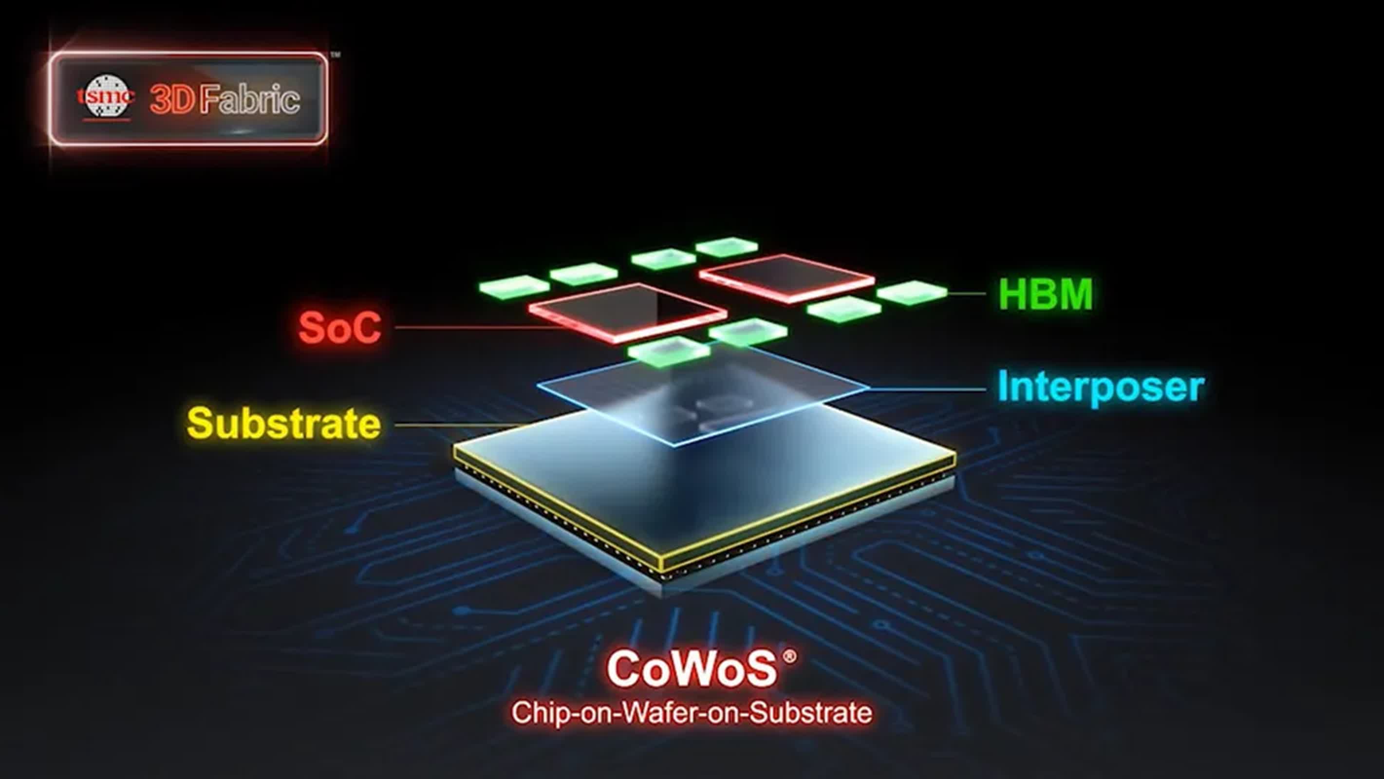
The big picture: The semiconductor industry is approaching a significant milestone as TSMC prepares to expand the physical scale of its chip packaging technology. At its recent North American Technology Symposium, the company detailed plans for a new generation of CoWoS (Chip-on-Wafer-on-Substrate) technology, enabling the assembly of multi-chiplet processors much larger than those currently in production.
Today’s high-end processors, especially those powering data centers and AI workloads, already rely on multi-chiplet designs to meet soaring demands for performance and memory bandwidth. TSMC’s current CoWoS solutions can accommodate interposers up to 2,831 mm², more than three times the size of a standard photomask reticle, which is limited to 830 – 858 mm² by EUV lithography constraints.
This technology is already being used in products like AMD’s Instinct MI300X and Nvidia’s B200 GPUs, which combine large compute chipsets with stacks of high-bandwidth memory.
However, as AI and high-performance computing applications continue to grow in complexity, the appetite for even more silicon is only increasing. To address this, TSMC is developing a new CoWoS-L packaging technology, set to launch as early as next year, supporting interposers as large as 4,719 mm² – about 5.5 times the reticle limit – and require substrates measuring 100×100 mm. This will allow up to 12 stacks of high-bandwidth memory, a significant step up from current capabilities.
TSMC projects that chips built with this technology will deliver more than three and a half times the compute performance of today’s leading designs, potentially meeting the needs of upcoming processors like Nvidia’s Rubin GPUs.
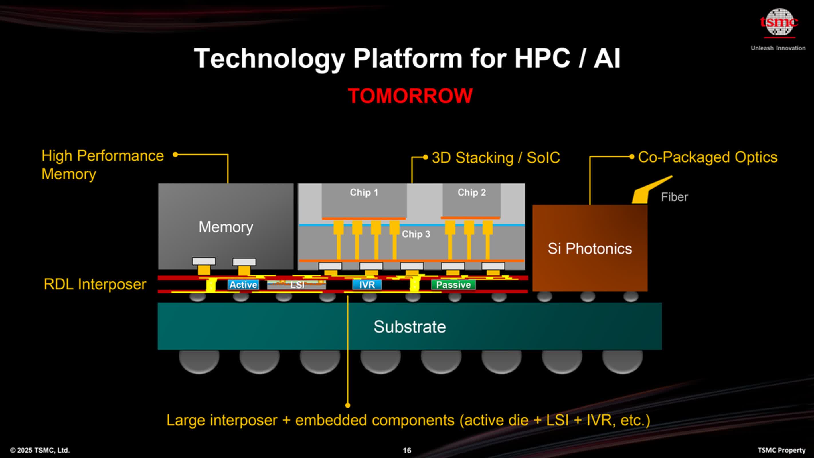
Looking further, TSMC plans to push the envelope with an even larger package: a 7,885 mm² interposer mounted on a 120×150 mm substrate, a footprint slightly bigger than a standard CD case. This represents a 9.5-fold increase over the reticle limit and nearly doubles the area of the company’s previous 8x-reticle package.
Such a massive assembly could host four 3D-stacked systems-on-integrated chips, twelve HBM4 memory stacks, and multiple input/output dies, setting a new benchmark for performance and integration.
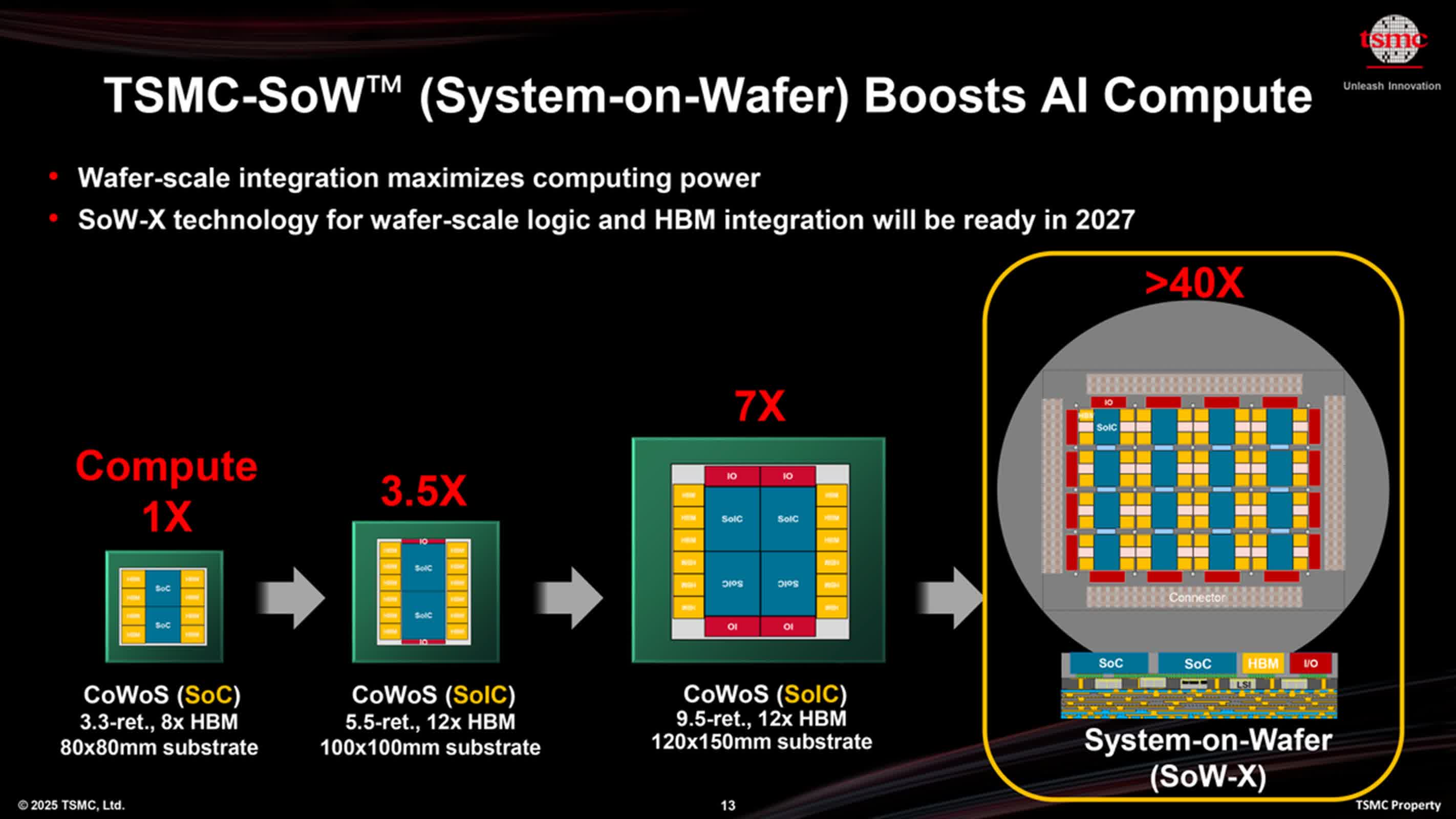
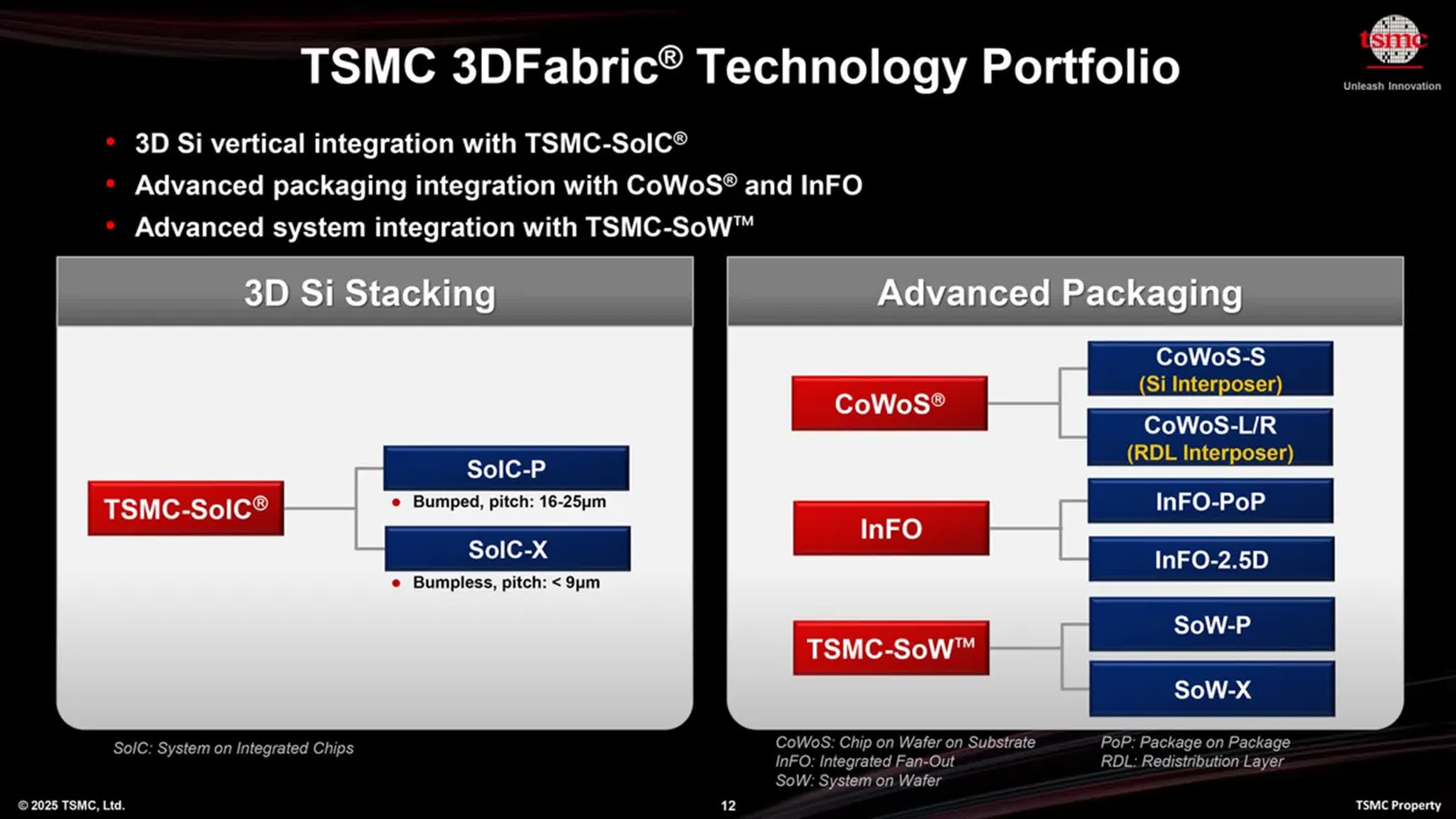
For customers with the most extreme performance requirements, TSMC is also offering its System-on-Wafer (SoW-X) technology, which enables the integration of entire wafers into a single chip. While only a few companies, such as Cerebras and Tesla, currently use wafer-level integration for specialized AI processors, TSMC anticipates broader adoption as the demand for super-sized chips grows.
The engineering challenges associated with these behemoth processors are considerable. Delivering power to large, multi-chiplet assemblies requires innovative solutions, as they can draw kilowatts of power, far beyond what traditional server designs can handle.
To tackle this, TSMC is integrating advanced power management circuits directly into the chip package. Using its N16 FinFET technology, the company embeds monolithic power management ICs and on-wafer inductors into the CoWoS-L substrate, allowing power to be routed efficiently through the package.
This approach reduces electrical resistance and improves power integrity, enabling dynamic voltage scaling and rapid response to changing workloads. Embedded deep trench capacitors further stabilize electrical performance, filtering out voltage fluctuations and ensuring reliable operation under heavy computational loads.
These advances reflect a broader shift toward system-level co-optimization, where power delivery, packaging, and silicon design are treated as interconnected elements rather than separate concerns.
However, the move to ever-larger chip packages is not without its complications. The physical size of the new substrates, particularly the 100×100 mm and 120×150 mm formats, is pushing the limits of existing module standards such as OAM 2.0, and may require new system and board design approaches.

Thermal management is another critical challenge. As processors grow in size and power consumption, they generate enormous amounts of heat. Hardware manufacturers are exploring advanced cooling techniques, including direct liquid cooling and immersion, to keep these chips running efficiently.
TSMC has already worked with partners to develop immersion cooling solutions for data centers. These solutions can significantly reduce energy consumption and stabilize chip temperatures, even under intense workloads. However, integrating these cooling technologies directly into chip packages remains a challenge for the future.
Source link