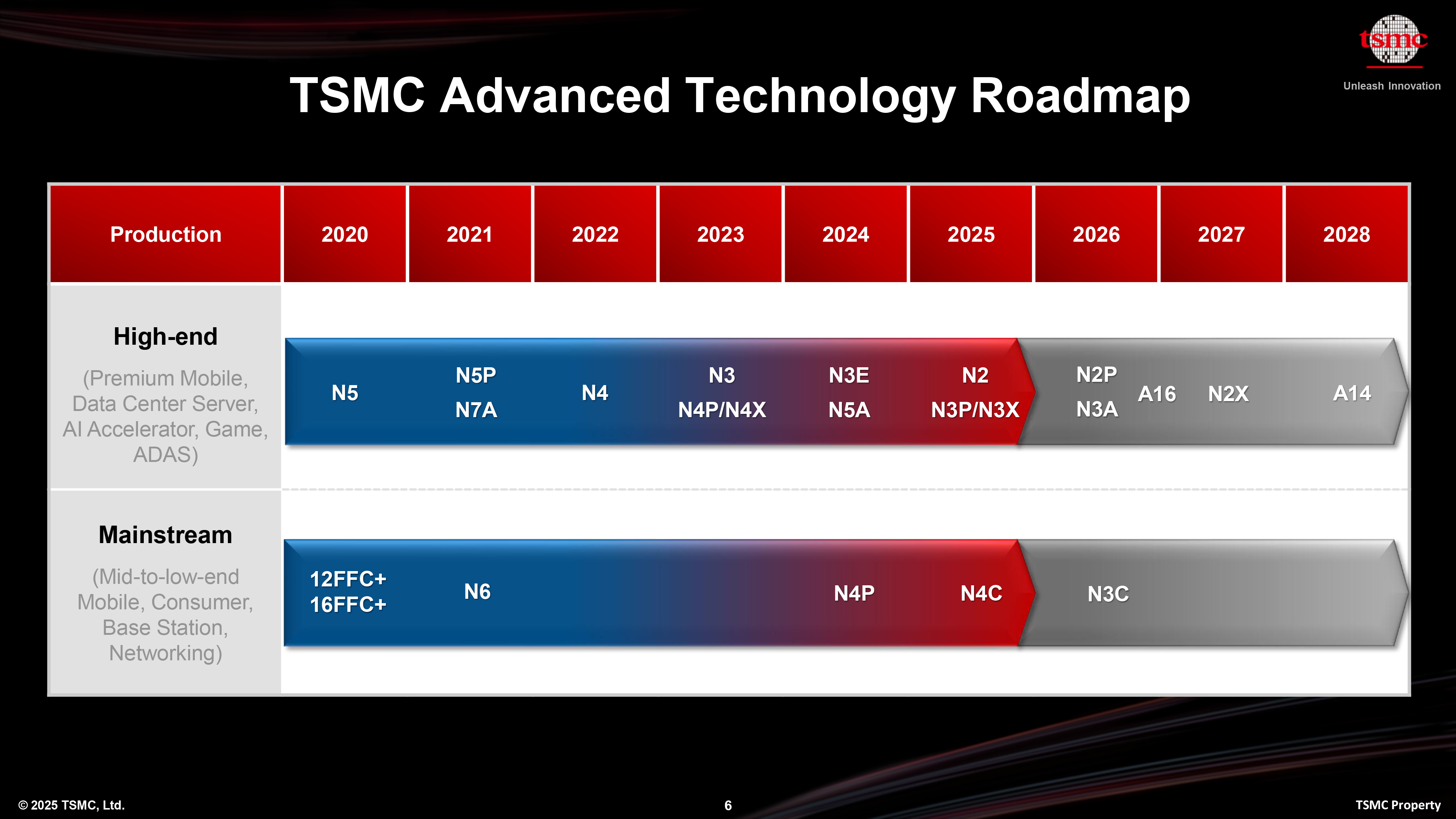
In brief: TSMC has announced that its A14 (1.4nm-class) chip manufacturing process will enter production in 2028, following the rollout of its 2nm technology later this year and building on its current lineup of 3nm-class chips. The company says the A14 node represents a significant leap in both performance and efficiency.
The roadmap was unveiled this week at the North American Technology Symposium. As part of the announcement, TSMC revealed plans for an intermediary A16 node, slated for release in late 2026. This node will serve as a stepping stone toward the more transformative A14 process.
A key highlight of the A14 generation is NanoFlex Pro, an enhanced transistor architecture that enables chip designers to fine-tune configurations for optimal power, performance, and area based on the specific requirements of each application.

While TSMC hasn’t disclosed all the technical details of NanoFlex Pro, it’s expected to build on the company’s existing FinFlex architecture, which allows designers to combine different standard cell types – such as high-performance, low-power, or area-efficient cells – within a single block. NanoFlex Pro may offer even finer-grained control, potentially at the transistor level, or introduce smarter design tools to accelerate chip optimization.
Meanwhile, production is already ramping up for TSMC’s third-generation 3nm-class process, N3P, which officially entered mass production in Q4 2024. As an optical shrink of N3E, N3P is now powering high-performance chips for clients in both data centers and advanced consumer technology sectors.
Next in line is N3X, expected to reach volume production in the second half of this year. Tailored for maximum frequency, N3X delivers an additional five percent performance gain over N3P and supports voltages up to 1.2V, an unusually high threshold for 3nm nodes. This makes it particularly well-suited for client CPUs and AI accelerators that prioritize raw speed over power efficiency.
TSMC Deputy COO Kevin Zhang noted that while smartphones once led the way in adopting new nodes, the AI boom has reversed that trend. Today, AI chipmakers are the first to embrace the latest and most advanced process technologies.
With N3P in full production, N3X on track, and A14 on the horizon, TSMC is doubling down on its strategy of offering multiple node enhancements to extend the lifecycle of its leading-edge fabs and customer IP. All of this is underpinned by a massive $40 billion in capital expenditures for 2025, reinforcing the foundry’s position as the premier choice for the world’s most advanced semiconductors.
Source link