[ad_1]
PCI Express is a technology that consistently makes headlines, with new specifications boasting ever-improving performance regularly appearing in the news. It may come as a surprise, then, to learn that it has been around for 20 years! With no signs of being replaced, the technology must be something special to last this long.
If you’re wondering exactly what it does and how PCI Express has remained a staple part of every home computer for two decades, then you’ve come to the right place.
Before Express and before PCI
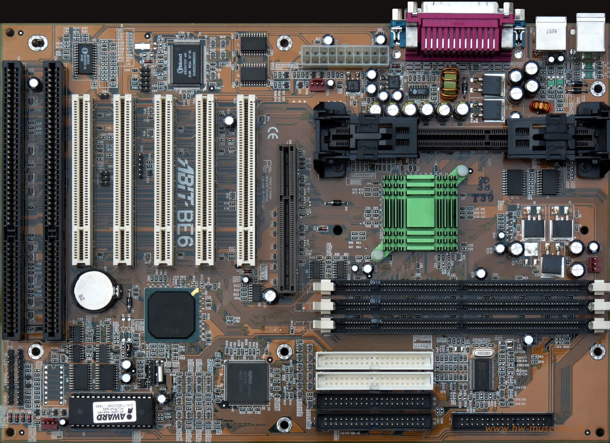
Let’s start by heading back to the 1980s when computer motherboards were festooned with dozens of chips and a multitude of peculiar expansion slots for adding extra cards. Two types primarily dominated the domestic scene: IBM’s ISA bus (Industry Standard Architecture) and VLB (VESA Local Bus) from the Video Electronics Standards Association. The latter was superior to the former, as it could run considerably faster and transfer more data per second, offering up to 10 times more bandwidth.
By the time the next decade arrived, the need for better-performing expansion buses drove Intel to develop something that would eventually replace them both – the PCI bus (Peripheral Component Interconnect). Released in 1992, it initially looked slower than VLB, as it was designed to run at a fixed 33 MHz (a later revision of the specification did permit 66 MHz, but consumer PCs never really supported this). In contrast, the older bus ran at the same clock as the CPU’s front side bus (FSB), allowing VLB to reach 40 or 50 MHz, depending on the central processor.
However, VLB wasn’t always stable at that rate and had worse latencies than PCI. A typical VLB expansion slot was also much larger than a PCI one. Despite these advantages, PCI took some time to gain traction in the motherboard industry, particularly in the workstation and server markets.
At that time, home PC users typically did not have many expansion cards, or any that placed significant demands on the bus. However, this changed when the 3D graphics card industry took off, and the best cards featured PCI connectors. As a result, motherboards began to favor the new bus over the old ones. As these graphics accelerators grew in power and games capitalized on this, the limitations of the PCI bus became apparent.
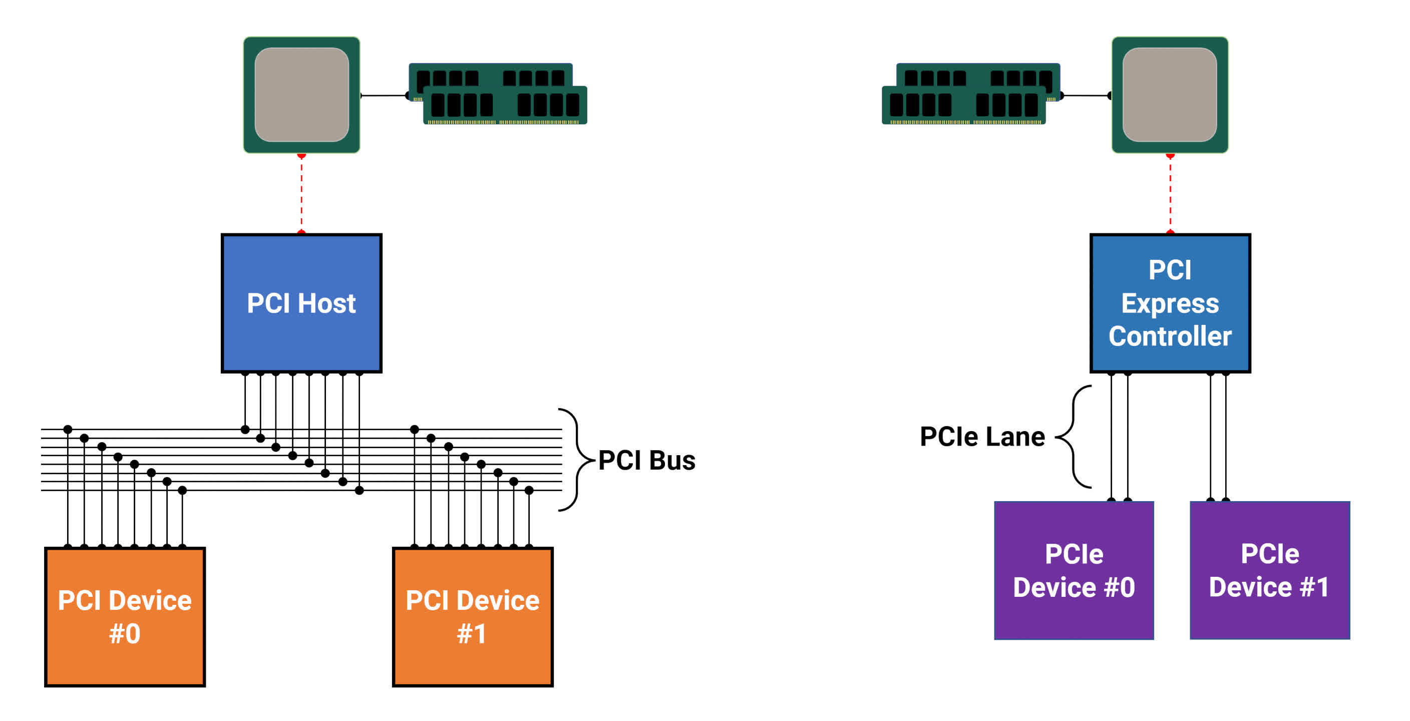
Like ISA and VLB before it, PCI was a parallel data bus – this meant that all cards in PCI expansion slots used the same bus and had to take turns to transmit and receive data. For graphics cards, this could be problematic, as they could easily hog the bus. Intel addressed this issue by developing the Accelerated Graphics Port (AGP) in 1997, which provided a specialized PCI bus exclusively for the graphics card.

As the old millennium transitioned into a new one, the demand for an even faster bus was mounting. Shortly after Intel launched the PCI bus, it formed a Special Interest Group (PCI-SIG) to support motherboard and expansion card vendors in ensuring their hardware complied with the specifications. By the early 2000s, this group comprised hundreds of members, and five of them (Compaq, Dell, HP, IBM, and Microsoft) collaborated with Intel on a replacement for PCI.
Codenamed 3GIO (3rd Generation I/O), the PCI-SIG announced the fruits of its labors in April 2002, introducing the new technology as PCI Express.
PCI vs PCI Express
Despite sharing the same name, PCI Express (often simply called PCIe) and PCI buses have little in common. The most significant difference is that PCIe is a point-to-point system – only one device uses the bus and doesn’t share it with anything else. In some ways, this might seem like PCIe is merely an upgraded AGP, but there’s also a significant difference in how data is transmitted.
While PCI and AGP use parallel data communication, sending and receiving multiple bits of data simultaneously, PCIe employs serial communication, sending just one bit per cycle. This approach eliminates the problem of clock skew, which can occur in parallel communication and lead to issues, ultimately allowing PCIe to run at much higher clock speeds.
PCI has an absolute limit of 66 MHz (an extended version, PCI-X, could reach 533 MHz), while the slowest clock speed for PCI Express is an astonishing 1250 MHz.
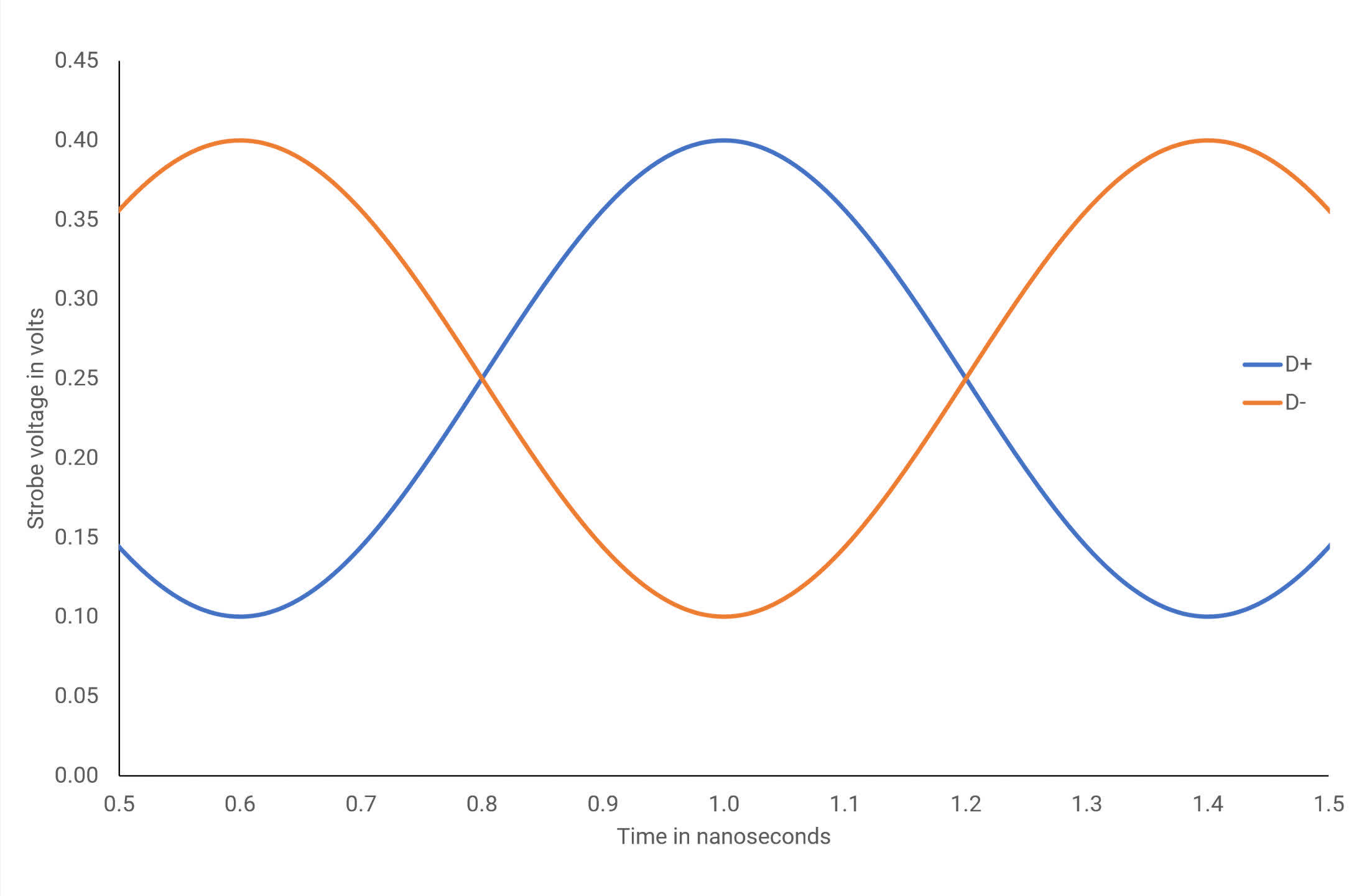
This speed is achieved through the use of low voltage differential strobes (LVDS) – a pair of signals, 180 degrees out of phase, operating at a fraction of the voltage that PCI and AGP use.
The serial nature of PCI Express also significantly reduces the number of wires/traces required for data transfer, with 32 needed for PCI and just four for PCIe. Technically, only two are required, one for each strobe, but since PCI Express is fully duplex, sending information in both directions simultaneously, a double set of paired strobes is always used.
This group of four wires is better known as a PCIe lane, and the specification indicates the number of lanes used via a multiplier, e.g., x1 is one lane, x4 is four, x16 is sixteen lanes, and so on.
With the way the LVDS system works, a single-lane PCIe bus can transmit data at a minimum rate of around 200 MB/s in one direction. On paper, it should be higher than this, but the transmitted information is encoded and sent in 8-bit packets, with each successive packet sent down a successive lane. As a result, the actual data rate is always lower due to the additional bits required for encoding.
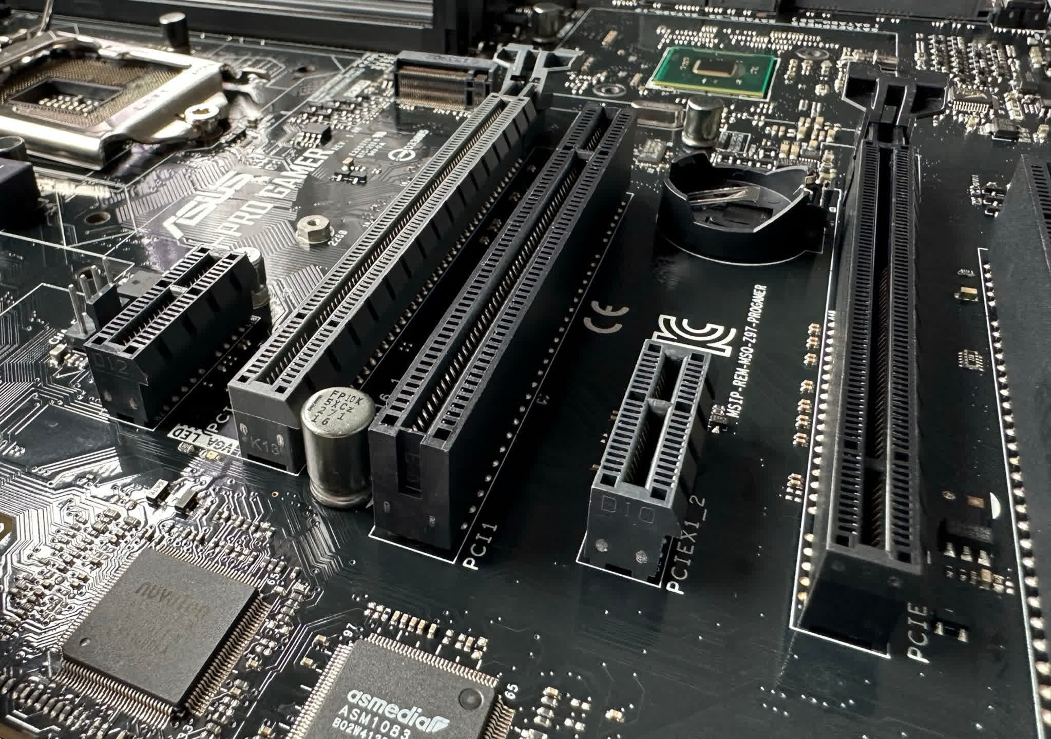
The combination of serial communication and packet-based data transfer also means that relatively few pins in the slot connection are required for managing everything. The minimum for any PCI Express device is 18, although not all of them need to be used. In contrast, PCI slots require at least 56, which inevitably takes up more space, regardless of how compactly it is arranged.
That said, a PCIe x16 slot is noticeably longer than any standard PCI or AGP slot, but not as tall. In fact, regardless of the length of the PCI Express expansion slot, they are almost all the same width and height (those for graphics cards are sometimes a little taller) – longer slots simply accommodate more lanes for sending traffic. Everything related to power and system management is located in the first section of the slot, before the plastic notch.
The universal application of PCI Express
From the very start of its design, PCIe was created with the aim of making the scope for use cases as broad as possible. To that end, engineers made the system backward-compatible with PCI, although only in terms of software. This meant that developers didn’t have to worry about rewriting their software to recognize and access any devices using the PCI Express bus – in theory, it would simply work.
To get the most out of the new system, hardware vendors designed their products to fully incorporate PCI Express into a variety of components and structures. Although this took the better part of a decade to achieve, the high-speed, universal bus eventually replaced the bus used for connecting the CPU to the rest of the motherboard, as well as all the expansion card slots.
Both AMD and Intel had developed their own point-to-point, ultra-fast connection systems for CPUs, with the former introducing HyperTransport several years before Intel employed its QuickPath Interconnect technology to connect central processors to the Northbridge chip, which traditionally handled data flows for the system memory and graphics card slot. Eventually, this chip would disappear altogether, being embedded into the CPU itself, and both companies switched to using PCI Express to connect to the remaining motherboard chip – the Southbridge.
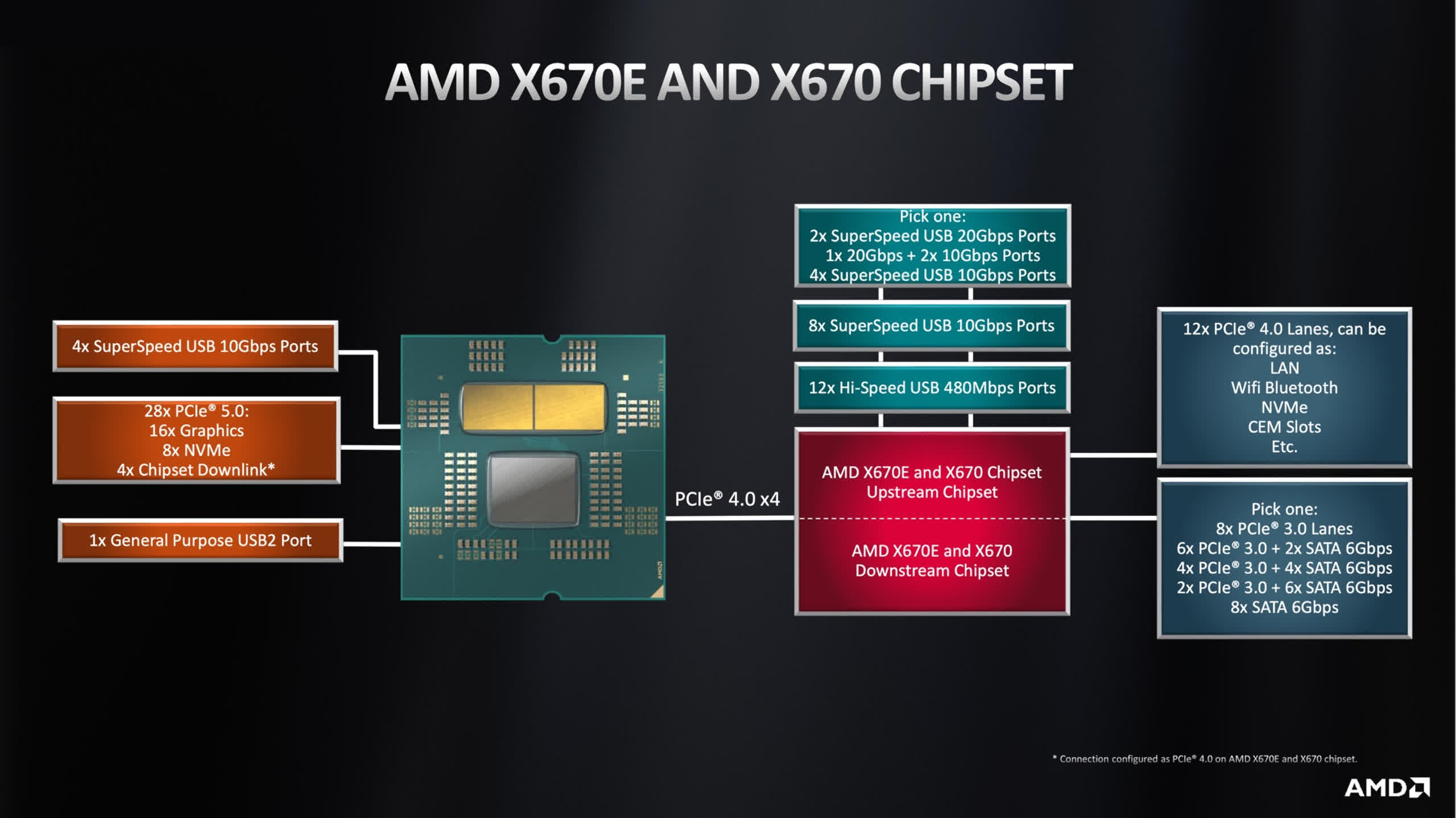
Choose any CPU and motherboard from AMD and Intel today, and you’ll see that the processor and Southbridge (now called the PCH by Intel and simply chipset by AMD) both feature large PCI Express controllers, with numerous lanes.
For example, AMD’s Ryzen 9 7950X processor and X670E motherboard chip boast 28 and 20 PCIe lanes respectively. In the case of the Ryzen CPU, they are allocated to dedicated roles: 16 for the graphics card slot, 8 for two storage drives, and the remaining 4 to communicate with the motherboard. The lanes in the X670E chip, however, can be used in various data scenarios, such as Ethernet, WiFi, and Bluetooth adapters, as well as expansion slots and storage drives.
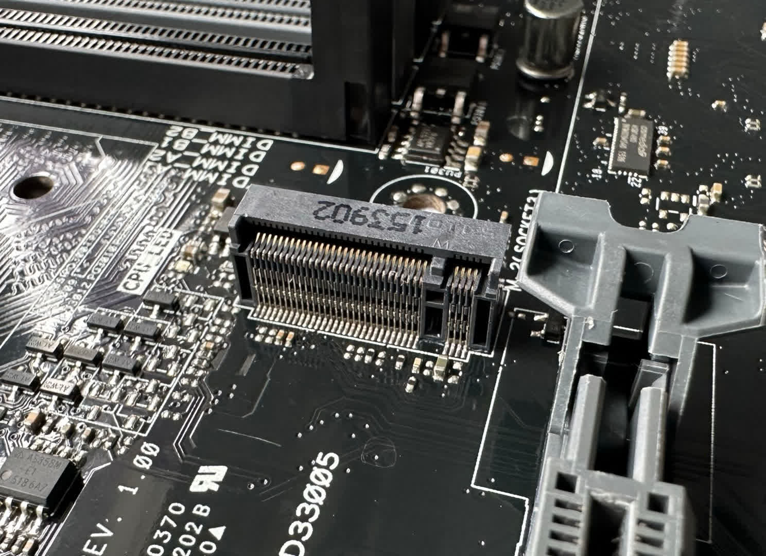
The adaptability of PCI Express is especially important for storage – today’s motherboards feature two primary sockets for connecting hard disk and solid-state drives (HDDs & SSDs), namely SATA and M.2 sockets (the latter shown above). If we look at Gigabyte’s X670E Aorus Xtreme model, you’ll find a total of three expansion slots, four M.2 sockets, and six SATA sockets. All of these use PCI Express!
However, with a fixed number of lanes in the CPU and chipset, they can’t all be used simultaneously, which is typically the case for most motherboards today. Deciphering which combinations of graphics cards, add-in cards, and storage drives will work is no simple task, unfortunately.
Modern PCs boast a vast array of sockets for connecting various devices, but behind the scenes, it’s a PCI Express bus handling the data transfer for the majority of them (the rest being USB).
How PCI Express has stayed up-to-date
Hardware has become ever more capable over the years, and applications and games have demanded increasingly more of it as well. Naturally, PCI Express has been regularly updated since its inception to keep up with bandwidth requirements.
A significant constraint on the updates was the requirement for full backward compatibility. For example, a PCIe 3.0 device must be able to work in a PCIe 5.0 slot. This created a couple of glitches, which we will cover in a moment.
Since the initial release in 2003, PCI-SIG has issued eight updates to the specifications, with major revisions featuring faster data transfer rates, as well as improvements to the encoding scheme employed (to reduce the loss in bandwidth) and signal integrity. Minor revisions focused on refining power management, control systems, and other aspects.
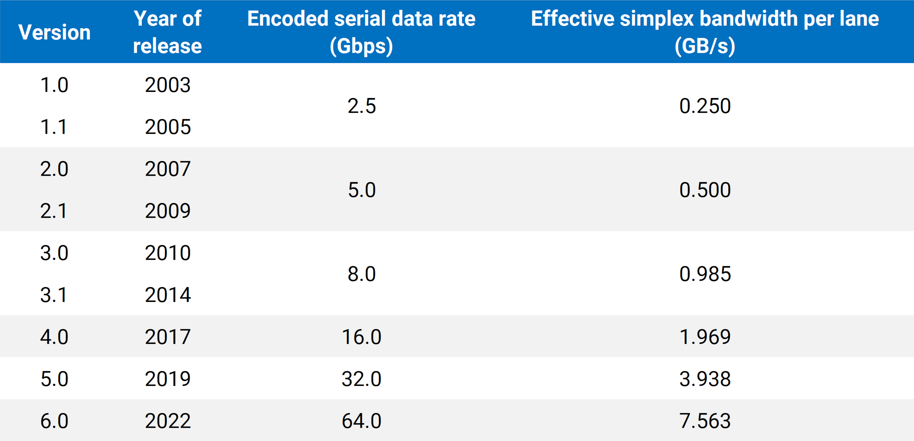
During the development of each revision, the relevant members of the PCI-SIG work on feasibility studies to determine what speeds and features can realistically be mass-manufactured while retaining low costs. This is why, for version 3.0, the clock rate of the strobes was only increased by 60% rather than doubling them, as was done with the previous version.
Version 3.0 introduced a more effective encoding scheme (specifically, 8b/10b was used for 1.0 and 2.0, whereas 128b/130b was used for 3.0 through to 5.0), which is why the effective bandwidth is higher relative to the clock speed. If no encoding was needed, PCIe 1.0 would have an effective bandwidth of 0.313 GB/s.

For version 6.0, the signaling method switched from NRZ to PAM4 (as used in GDDR6X memory) and encoding was dropped in favor of various error correction systems.
To put the bandwidth figures into perspective, a single stick of DDR4-3200 RAM has a peak throughput of 25 GB/s, so four lanes of PCIe 6.0 would match this. That might not sound particularly impressive, but for a general-purpose communication bus used in everyday PCs and other computing machines around the world, it’s a remarkable improvement.
But why are PCs only just adopting PCIe 4.0 and 5.0 now, when the specification for the former was released back in 2017 (and 5.0 was two years after that)?
It comes down to matters of need and cost. As things currently stand, PCs have more than enough bandwidth for moving data around internally, and aside from video games, there isn’t much scope for a home computer to need the likes of PCIe 6.0 just yet.
However, in the server world, system designers will gladly take all the bandwidth they can get, and it’s in that area that we’re likely to see the most recent specification being first used.
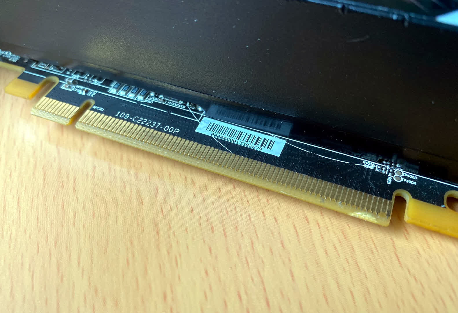
Not every update release has been smooth sailing, though, and electrical power has been a perennial problem for the system. No matter what size of PCIe slot a device uses, they all come with a handful of +3.3 V and +12 V pins for supplying current to run the device.
From the very first PCIe version, the combined current limit on the +3.3V pins is 3 A, and depending on what size add-in card is used in the slot, up to 5.5 A for the +12 V pins.
That means for a full-length x16 card, the device is limited to a power consumption of 75.9 W, which was enough for the vast majority of graphics cards at that time. There were exceptions, of course, such as Nvidia’s GeForce 6800 Ultra, released in the summer of 2004.
Its maximum power demand was a little over 80 W, more than the slot could provide, and the solution came in the form of an AMP 1-480424-0 – better known as a Molex connector. Depending on the manufacturer of the part and the quality of the cables used, that could provide an additional 130 W of power.
However, this addition wasn’t part of the PCIe specification, so PCI-SIG created its own solution in the form of two designs – one containing 6 pins for 75 W and the other sporting 8 pins for 150 W.
More recently, PCI-SIG approved a 16-pin design, with the majority of the development coming from Nvidia (and is currently only used by them), which has a 600 W limit. The 12VHPWR connector has not been without controversy, and it remains to be seen if AMD and Intel will ever adopt the mechanism.
What’s next for PCIe?
With version 7.0 scheduled for release in 2025, PCI-SIG shows no signs of slowing down the development of technology, nor is it looking to replace it with anything considerably different any time soon.
The next update is expected to see another doubling in the data transfer rate, although the group members may reduce the increase a bit if they feel it’s not financially sensible to go with 128 Gbps. Home PCs aren’t likely to see such speeds implemented for a good number of years, probably not until the mid-2030s, given the current adoption rate of PCIe 5.0, let alone the newer spec.
But let’s pretend that 7.0 is out now and every new piece of hardware is ready and able to use it – just what benefits could this bring?
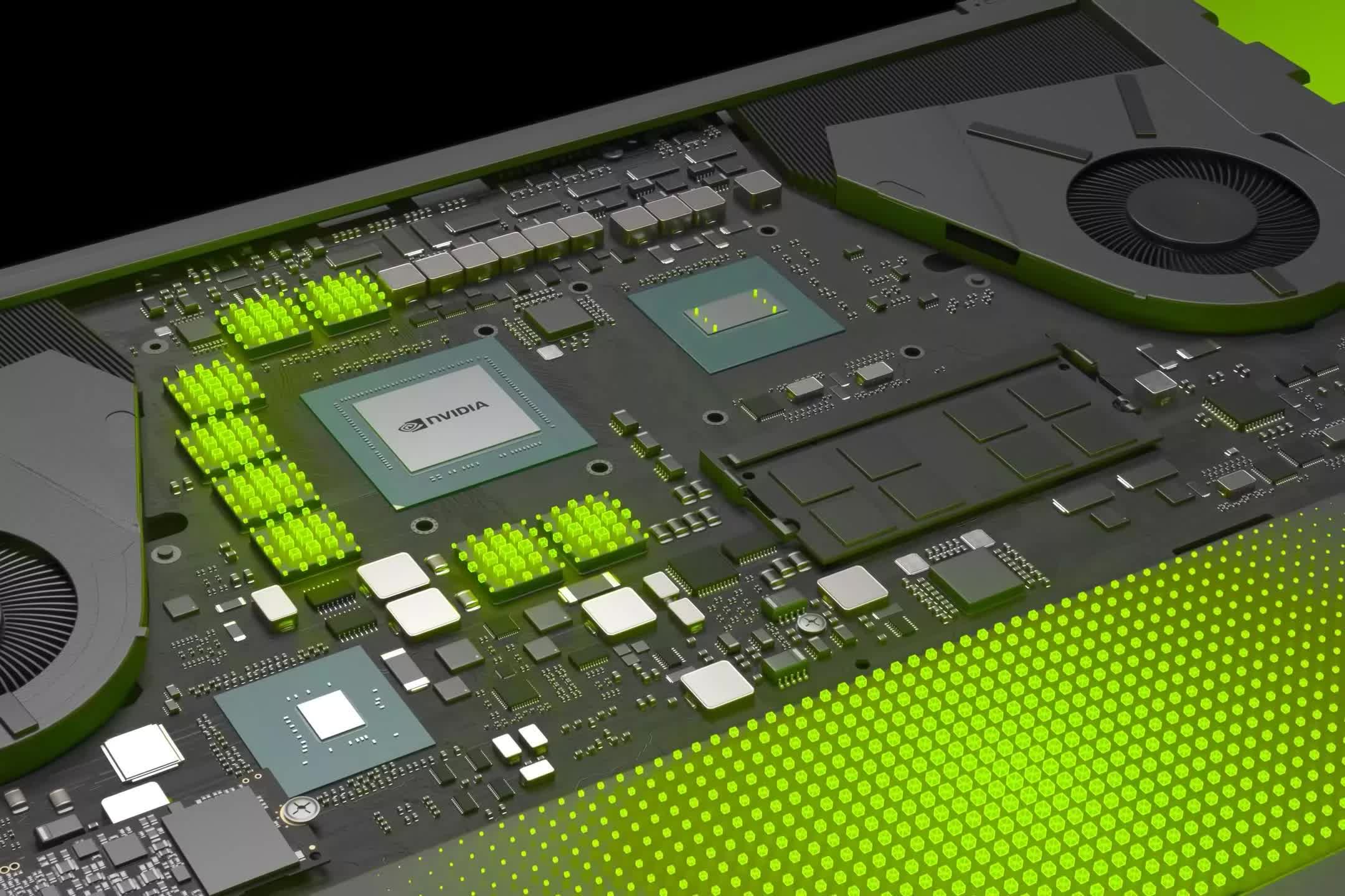
For a start, graphics cards would have a connection to the PCIe controller in the CPU sporting a bandwidth of 242 GB/s. That’s roughly the same amount of memory bandwidth that you’d find on an AMD Radeon RX 6600 or Nvidia RTX 3050. You might think that this means discrete GPUs found in laptops could just use system memory, instead of needing their own RAM, saving money and space.
But the PCIe controller still has to communicate with the CPU’s memory controller to access system RAM, and even ultra-fast DDR5, such as DDR5-7200, only offers around 58 GB/s per DIMM. In other words, the GPU is still going to be restricted by using system memory, despite the speed of the PCIe 7.0 bus.
So if GPUs are not going to benefit, what about storage drives? At the moment, the fastest NVMe M.2 SSDs only just reach the limits of a PCIe 4.0 x4 bus, and even then, only in very specific and brief circumstances. Faster drives will appear over time, of course, but there are faster versions of PCI Express, too.
Today’s desktop CPUs connect to the motherboard chipset via a PCIe bus, with AMD using v5.0 in its latest Ryzen 7000 series and Intel using its own system called Direct Media Interface (DMI) that’s PCIe in all but name.
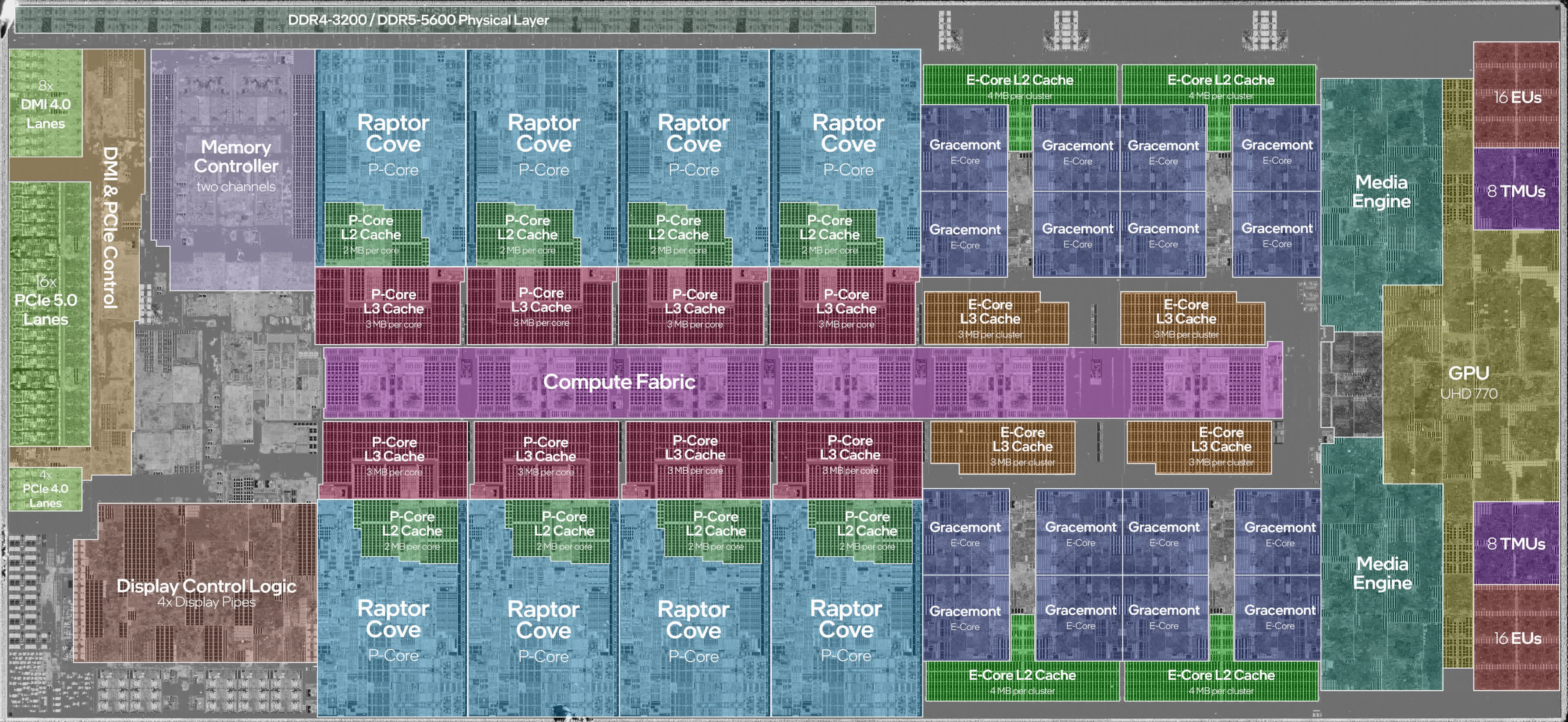
There’s no indication from either vendor that this link restricts the performance in any way – if it was, CPUs would be using more lanes, as the amount of die space needed for each one is tiny, compared to the rest of the chip.
This may all lead you to think that the constant updates to the PCI Express specification are a waste of time, but it’s about getting all hardware vendors to agree on a standard early enough to give them sufficient time to develop products and manufacturing methods for them.
PCIe is now as ubiquitous as USB and just as its serial cousin is now the universal backbone for moving data about with peripherals, PCI Express is the norm inside a computer. The PC industry depends on PCI Express to meet every possible need, all while being cost-effective.
Specialized applications, such as AI, data, and compute servers will always go their own way and sport technologies unique to their needs, but when it comes to the everyday PC and most workstations, PCI Express is the king of connections and will be for decades to come.
PCIe shopping (of a few cool and affordable gadgets):
- Samsung 970 Evo Plus 2TB SSD on Amazon
- TP-Link AC1200 PCIe WiFi card on Amazon
- 4-Port PCIe to USB 3.0 controller card on Amazon
- Dual HDMI 1080p PCIe video capture card on Amazon
- PCIe 4.0 X16 riser cable on Amazon
Keep Reading. Explainers at TechSpot
[ad_2]
Source link
