
[ad_1]
Forward-looking: Nvidia’s Ampere architecture has finally arrived even though we’re still months away from consumer cards we can use in our gaming PCs. The company says this is a significant leap over the Turing architecture: the new A100 chips are based on a 7nm process and is as much as 20 times faster than the Tesla V100.
Ampere hype had been at the highest levels as of late, with many getting excited about Nvidia’s next-gen GPU architecture and the improvements it may bring. But when CEO Jensen Huang was shown in a video pulling a very heavy piece of kit from his oven, it didn’t look like consumer-grade hardware.
Today, Nvidia officially unveiled its next-generation Ampere GPU architecture, which is coming to servers and supercomputers first in the form of A100, a GPU designed for cloud computing, AI, and scientific number crunching. For those of you expecting the GeForce RTX 3080 to make an appearance, that’s still months away.
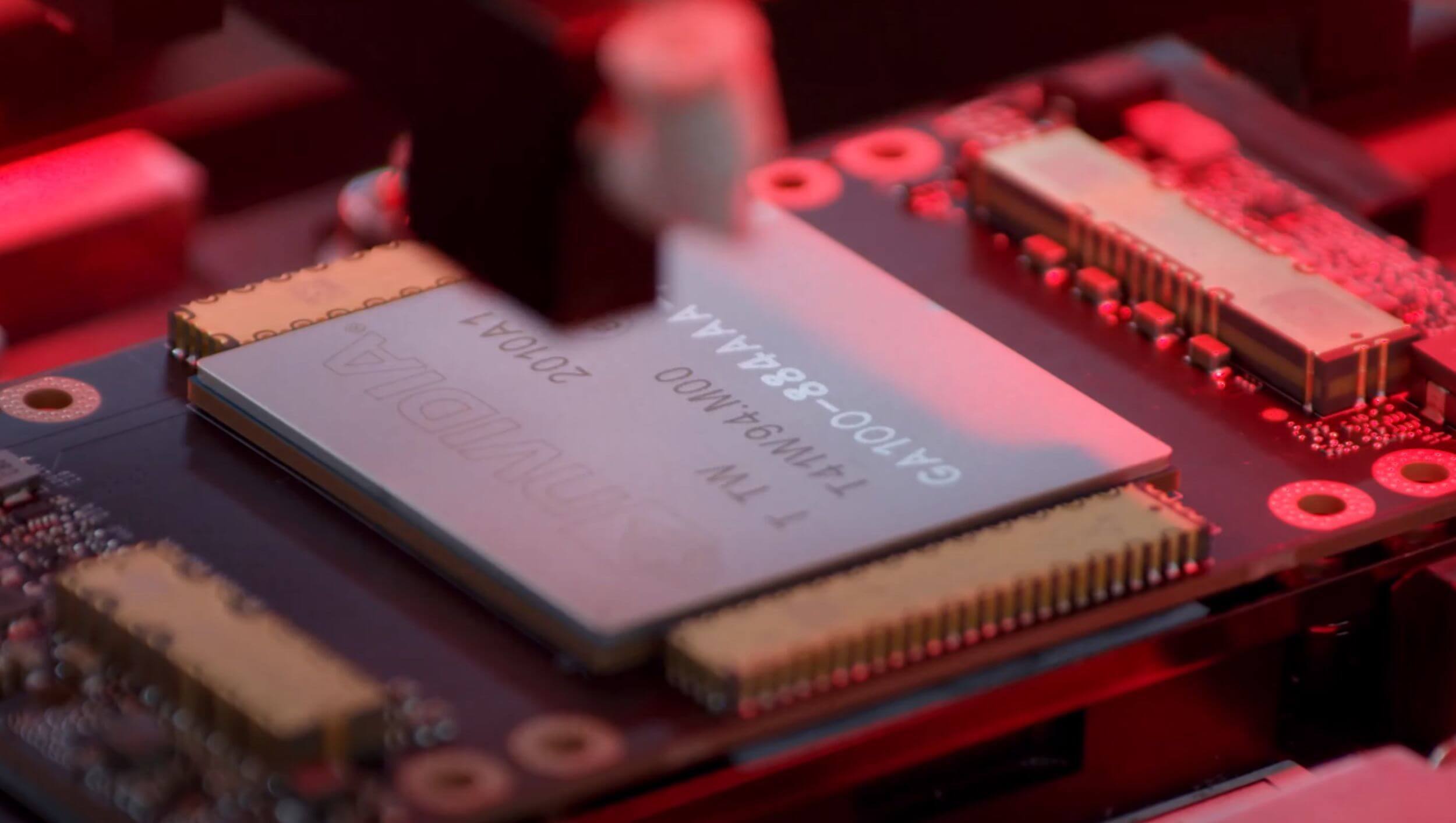
The company says the A100 is the biggest generational leap for its GPUs, with 20 times the speed of the previous Volta-based solution and third-generation Tensor cores. This is a silicon beast that has 54 billion transistors and offers 6,912 CUDA cores. And, as expected, Nvidia’s new Ampere GPU is built on a 7nm process.
One of the biggest advantages of the new chip is that it can be used to reduce costs for big data centers. Nvidia says that a system that costs $11 million today and requires 25 racks of servers and 630 KW of power can be replaced by an Ampere system that fits in a single rack, costs $1 million and takes 28 KW of power to operate.
Such a system is based on what Huang pulled out of his home oven — a monstrous HGX motherboard that packs in eight A100 GPUs along with 30,000 discrete components and a kilometer of wire traces. This makes it one of the most complex motherboards out there, and Nvidia uses it in the DGX A100 system that is able to deliver 5 petaflops of AI compute performance and 320 GB of GPU memory with 12.4 TB per second of bandwidth in a relatively small package that weighs 50 pounds.
As for the consumer-grade hardware based on Ampere, Huang explains that Nvidia will configure the chip a bit differently. For instance, the A100 was designed to be great on double-precision floating point compute, with most of the 54 billion transistors going towards Tensor cores and FP64 units to deliver 19.5 teraflops and 9.7 teraflops of performance, respectively. Consumer oriented Ampere GPUs will be biased towards graphics and less towards compute.
The GTC 2020 keynote and press releases reveal little about clock speeds, but we do know that Ampere cards will support PCIe 4.0, and the move to 7nm means Nvidia can pack a lot more RT cores for improved ray tracing performance. Judging from the DLSS 2.0 presentation, there are significant improvements on the software front as well.
[ad_2]
Source link
