
[ad_1]
In the world of computer chips, bigger numbers are often better. More cores, higher GHz, greater FLOPs, all desired by engineers and users alike. But there is one measure that’s hot news right now and the smaller, the better. But just exactly what is it and why it’s so important? Why is it measured in nanometers and why are we going all Sesame Street and bringing this article to you with the numbers 10, 7 and 5? Let’s take a journey into the world of process nodes…
Before we delve into things, it will be worth spending some time going through our recent look at CPU architecture. In part one, we covered the fundamental architecture of processors and in part two, we examined how engineers plan and design them.
The key section relevant to this article is the explanation of how computer chips are physically put together. You’ll want to read the section on photolithography carefully if you want an in-depth understanding of the manufacturing process, while in this feature we’ll focus more on this point that was briefly touched upon:
One of the biggest marketing terms associated with chip fabrication is the feature size.
In the chip industry, the feature size relates to something called the process node. As we mentioned in How CPUs are Designed, Part 3, this is a fairly loose term, as different manufacturers use the phrase to describe different aspects of the chip itself, but not so long ago it referred to the smallest sized gap between two sections of a transistor.
Today it’s more of a marketing term and not very useful for comparing production methods. That said, the transistor is a critical feature of any processor, as groups of them perform all of the number crunching and data storage done inside the chip, and a smaller process node from the same manufacturer is a very much desired thing. The obvious question to ask here is why?
Nothing in the world of processors happens instantly and neither does it take place without requiring a source of electrical energy. Bigger components take longer to change their state, signals take longer to travel, and more energy is needed to move electricity about the processor. Without trying to sound obtuse, bigger components also take up more physical space, so the chips themselves are larger.
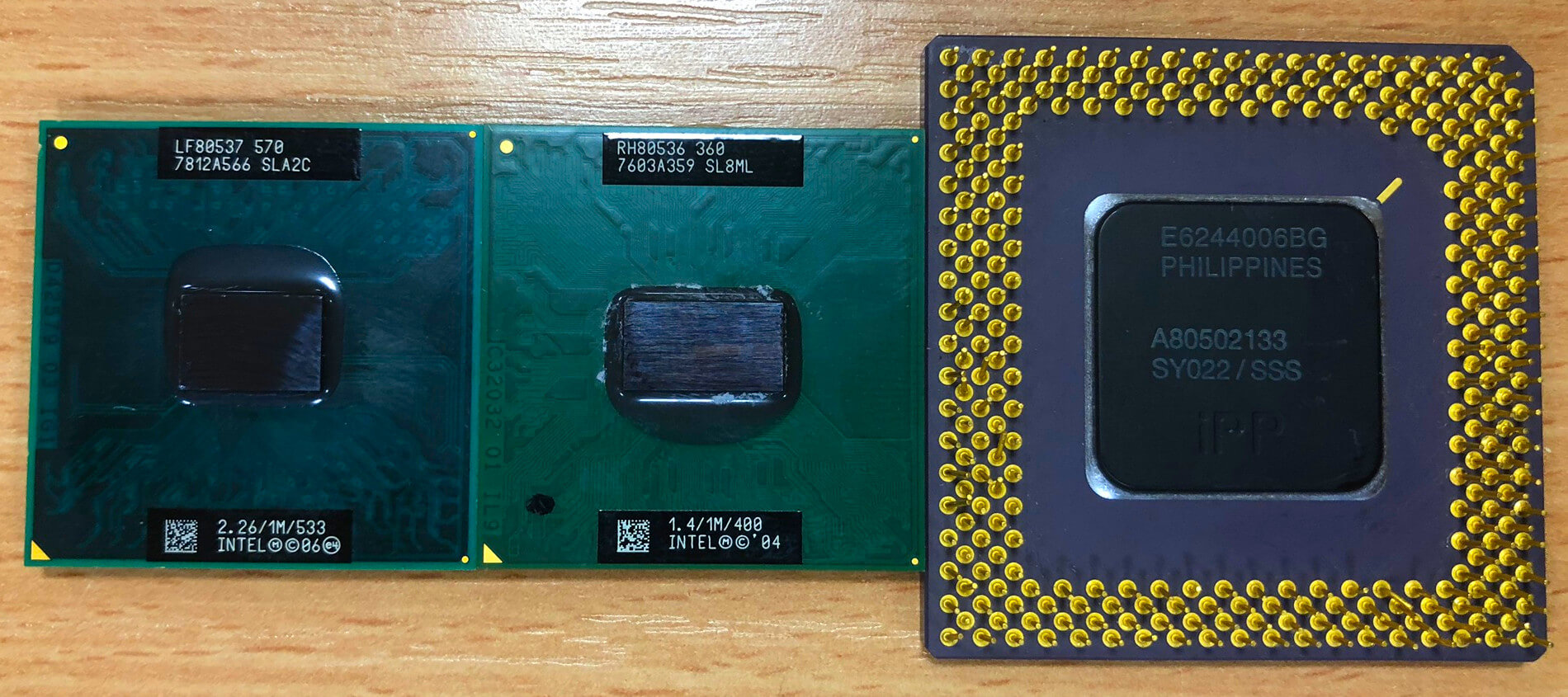
In the above image, we’re looking at three old Intel CPUs. Starting from the left, we have a 2006 Celeron, a 2004 Pentium M, and a really old Pentium from 1995. They have a process node of 65, 90 and 350 nm respectively. In other words, the critical parts in the 24 year old design are more than 5 times bigger than the 13 year old one. Another important difference is that the newer chip has around 290 million transistors packed inside, whereas the original Pentium has just over 3 million; almost a hundreds times fewer.
Although the reduction in process node is only part of the reason why the more recent design is physically smaller and has more transistors, it does play a significant role in Intel being able to offer this.
But here’s the real kicker: that Celeron only produces around 30 W of heat, compared to the Pentium’s 12 W. This heat comes from the fact that as electricity is pushed around the circuits in the chip, energy is lost due through various processes and the vast majority of it is released as heat. Yes, 30 is a bigger number than 12, but don’t forget that the chip has nearly 100 times more transistors.
So if the benefits of having a smaller process node results in smaller chips, touting more transistors that can switch faster — which gives us more calculations per second — and less energy lost as heat, it does beg another question: why isn’t every chip in the world using the smallest possible process node?
Let there be light!
At this point, we need to have a look a process called photolithography: light is passed through something called a photomask, which blocks light in some areas and lets it through in others. Where it passes through, the light is then heavily focused into a small spot and it then reacts with a special layer used in the manufacturing of the chip, helping to set out where the various parts are going to be.
Think of it being like an x-ray of your hand: the bones block the rays, acting as the photomask, whereas the flesh lets it through, producing an image of the internal structure of the hand.
Image source: Peellden, Wikimedia Commons
Light isn’t actually used — even for chips like the old Pentium, it’s too big. You might be wondering how on Earth light can have any size, but it’s in reference to wavelength. Light is something called an electromagnetic wave, a constantly cycling mixture of electric and magnetic fields.
Although we use a classic sine wave to visual the shape, electromagnetic waves don’t really have a shape. It’s more a case that the effect they generate when they interact with something follows that pattern. The wavelength of this cyclic pattern is the physical distance between two identical points: picture sea waves rolling onto a beach, the wavelength is how far apart the tops of those waves are. Electromagnetic waves have a huge range in possible wavelengths, so we put them together and call it a spectrum.
Small, smaller, smallest
In the image below, we can see that what we call light is just one tiny part of this spectrum. There are other familiar names: radio waves, microwaves, x-rays and so on. We can also see some numbers for the wavelengths; light is somewhere around 10-7 meters in size or roughly 0.000004 inches!
Scientists and engineers prefer using a slightly different method for describing lengths that small and it’s nanometers or nm for short. If we look at expanded section of the spectrum, we can see that light actually ranges from 380 nm to 750 nm.

Image source: Philip Ronan, Gringer
Go back up this article a touch and reread the part about the old Celeron chip — it was manufactured on a 65 nm process node. So how could parts smaller than light be made? Simple: the photolithography process didn’t use light, it used ultraviolet light (aka UV).
In the spectrum chart, UV starts at around 380 nm (where light finishes off) and shrinks all the way down to about 10 nm. Manufacturers such as Intel, TSMC, and GlobalFoundries use a type of electromagnetic wave called EUV (extreme UV), around 190 nm in size. This tiny wave not only means the components themselves can be created smaller, but the overall quality of them can be potentially better. This allows the various parts to be packed in closer together, helping to scale down the overall size of the chip.
The different companies offer various names for the scale of the process node they use. Intel snappily call their very latest one P1274 or “10 nm” for the general public, whereas TSMC simply call theirs “10FF.” Processor designers such as AMD create the layout and structures for the smaller process nodes, and then rely on the likes of TSMC to produce them, who ramped up their “7 nm” high volume production lines earlier this year. At this scale of production, some of the smallest features are just 6 nm across (the majority, though, are much bigger than this).
To get a sense of actually how small 6 nm really is, the silicon atoms that make up the bulk of the processor are spaced roughly 0.5 nm apart, with the atoms themselves being very roughly 0.1 nm in diameter. So, as a ballpark figure, TSMC’s factories deal with aspects of a transistor that cover less than 10 silicon atoms in width.
The challenge in aiming for atoms
Leaving aside the mind-boggling fact that chip manufacturers are working towards features being just a handful of atoms across, EUV photolithography has raised a whole bunch of serious engineering and manufacturing problems.
Intel has notably struggled to get its 10 nm production up to the same level as their 14 nm one and last year, GlobalFoundries stopped all development of their 7 nm and smaller production systems. Although Intel and GF’s problems may not be due to the difficulties inherent to EUV photolithography, they can’t be entirely unrelated.
The shorter the wavelength of an electromagnetic wave, the more energy it carries, which results in a greater potential for damage to the chip being manufactured; very small scale fabrication is highly sensitive to contamination and defects in the materials being used, too. Other issues, such as diffraction limits and statistical noise (natural variation in where the energy transferred by the EUV wave gets deposited into the chip layer), also conspire against the goal of achieving 100% perfect chips.
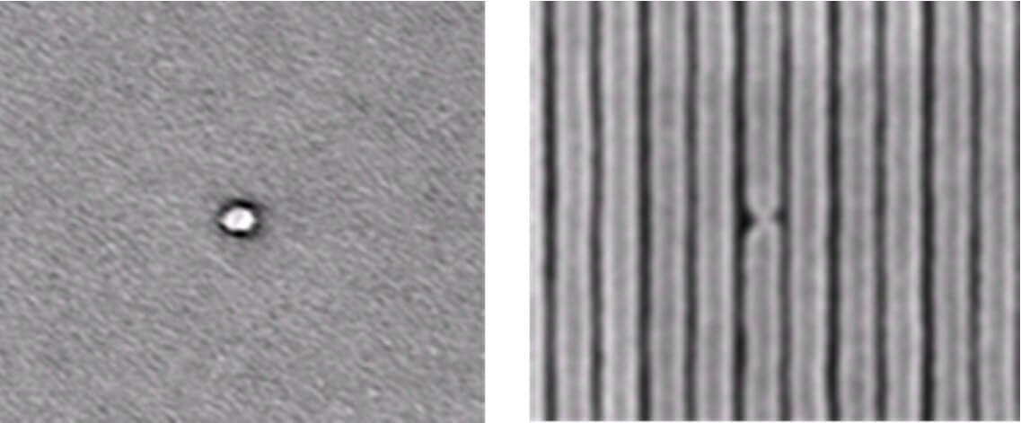
Two manufacturing defects in a chip. Source: Solid State Technology
There’s also the problem that down in the weird world of atoms, the flow of electricity and the transfer of energy can no longer be assumed to follow classical systems and rules. Keeping electricity, in the form of moving electrons (one of the three particles that make up atoms), flowing down conductors closely spaced together is relatively easy at the scale we’re used to — just wrap the conductors with a thick layer of insulation.
At the level Intel and TSMC are working at, this becomes much harder to achieve because the insulation isn’t really thick enough. For the moment, though, production issues are almost entirely related to the problems inherent to EUV photolithography, so it will be few years yet before we can starting arguing in forums that Nvidia handles quantum behaviour better than AMD or other such similar nonsense!
This is because the real problem, the ultimate reason behind the production difficulties, is that Intel, TSMC and all their fabricating chums are businesses, and they’re aiming for atoms for the sole purpose of generating future revenue. In a business research paper by Mentor, the following overview was offered as to how much more wafers cost for smaller process nodes.
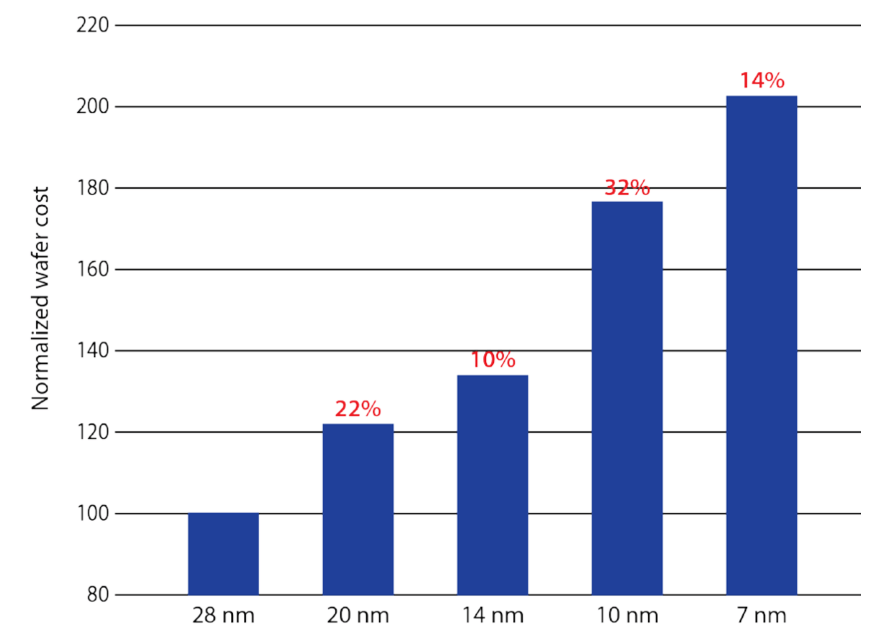
For example, if we assume the 28 nm process node is the same one that Intel used to manufacture their Haswell range of CPUs (such as the Core i7-4790K), then their 10 nm system is costing almost twice as much per wafer. The number of chips that each wafer can produce depends heavily on how large each chip is, but going with a smaller process scale will mean a wafer can potentially yield more chips to sell, helping to offset the increase in costs. Ultimately, though, as much of this cost as possible will be pushed to down onto the consumer by raising the product retail price but this has to be balanced against industry demand.
The rise in smartphone sales over the past few years, along with a near exponential growth in smart technology in homes and cars, has meant that chip manufacturers have been forced to absorb the financial hit from going to smaller process nodes until the whole system is mature enough to churn out high yielding wafers (i.e. those that contain as few defects as possible) in high volumes. Given that we’re talking about billions of dollars here, it’s a risky business and a good part of the reason why GlobalFoundries bailed out of the process node race.
Future prospects
If this all sounds somewhat doom-and-gloom, then we shouldn’t forget that the immediate future does look positive. Samsung and TSMC are not only running their 7 nm production lines to a healthy margin, in terms of volume and revenue, but chip designers are also planning ahead by using multiple nodes in their products. Of late, the most notable example of this has been AMD’s chiplet design on the recently released 3rd-gen Ryzen CPUs.
This top-end desktop PC processor will sport two chips manufactured on TSMC’s 7 nm node, and one 14 nm chip made by GlobalFoundries. The former will be the actual processor parts, whereas the latter will handle the DDR4 memory and PCI Express devices attached to the CPU. Assuming that this design works as intended (and there’s no reason to doubt that it should), then we will almost certainly see more companies following this multi-node setup.

The above image charts Intel’s process node changes over the past 50 years. The vertical axis shows the node size by factors of 10, starting all the way up at 10 000 nm. The chip giant has followed a rough node half-life (the time taken to reduce the node size by half each time) of 4.5 years.
So does that mean we will see a 5 nm Intel by 2025? Probably yes, despite their recent stumble with 10 nm. Samsung and TSMC have been forging ahead with their 5 nm research, so the future does look good for processors of all kinds.
They’ll be smaller and faster, using less energy and offer more performance. They’ll lead the way to fully autonomous cars, smartwatches with the power and battery life of current smartphones, and graphics in games beyond anything seen in multi-million dollar films from ten years ago.
The future is indeed bright, because the future is small.
[ad_2]
Source link

